
Sept. 17: Odisha is positioning itself to play a significant role in India’s semiconductor ecosystem, with advanced packaging emerging as one of the key focus areas under the India Semiconductor Mission 2.0.
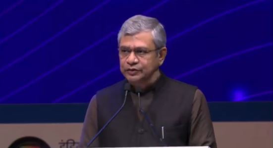
India Semiconductor Mission 2.0 also has advanced packaging as one of the focus pillars.
Odisha already has an edge with India’s 1st Advanced 3D Chip Packaging Plant being built in the state. #SEMICONIndia2026 pic.twitter.com/xufqVLOA0C
— E&IT Department Odisha (@EIT_Odisha) September 17, 2026
The Odisha Electronics & Information Technology (E&IT) Department, in a post on social media, highlighted the state’s existing presence in advanced semiconductor packaging and pointed to the development of what it described as India’s first advanced 3D chip packaging plant in Odisha.
Advanced Packaging Among Key Focus Areas
The department said advanced packaging is among the focus pillars of India Semiconductor Mission 2.0, underlining the growing importance of packaging technologies in the semiconductor value chain.
Odisha said its ongoing project in advanced 3D chip packaging gives the state an existing base as it seeks to attract further investments in the semiconductor sector.
Push To Build Semiconductor Ecosystem
The state government has been highlighting electronics and semiconductor manufacturing as emerging areas for industrial investment. The focus forms part of Odisha’s broader efforts to diversify its industrial base and attract technology-intensive projects.
The E&IT Department shared the update in connection with SEMICON India 2026, highlighting Odisha’s semiconductor ambitions and its positioning within India’s expanding chip manufacturing ecosystem.
The state is expected to continue its investment outreach to semiconductor companies and technology firms as India expands domestic capabilities across chip design, manufacturing and advanced packaging.
Leave a Reply